Current Ripple Factor of a Buck Converter
Abstract
Inductor and capacitor forms a low-pass filter in a buck converter. The corner frequency the LC filter is always designed to at low frequency to attenuate switching ripple. As a rule of thumb, current ripple of inductor is always designed to be around 30% of average inductor current. In this design note, a theoretical derivation of ripple current to average current ratio, also called ripple factor, is introduced to get inductor size equation. By applying area-product (AP) method of inductor design, an optimal range of ripple factor can be obtained, which is helpful for capacitor design as well as the total converter design.
Introduction
Buck converters are widely applied in lots of voltage step-down applications, such as on-board point-of-load converters. Basically, a power switch and a free-wheeling diode chop the dc input voltage to a rectangular waveform, then a low-pass LC filter sieves the high-frequency switching ripple and noise to get a almost pure dc voltage in the load terminal. Figure 1 shows a typical buck converter.
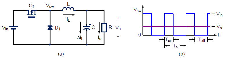
Figure 1. (a) A typical Buck converter, (b) Switching voltage.
When power switch Q1 turns on, the free-wheeling diode D1 is reverse bias. The input current goes through LC filter to load directly. When Q1 turns off, D1 is forward biased by inductor current iL. Switching voltage waveform shown as in Figure 1(b) is pulsating rectangular. After LC filtering, assuming corner frequency of LC is much lower than switching frequency, output voltage appears almost pure dc.
It can be understood the higher the inductance L is, the lower the capacitance C leads the same output voltage ripple. However, too big inductor causes high volume and high cost. While too low inductance causes big output capacitor. It is not purely a design trade-off problem. Let’s think about the waveforms of inductor current in steady state.
When power switch is at ON state, the voltage across inductor is voltage difference between input and output voltage.

The current will increase linearly from initial iL(0),

When power switch is at OFF state, inductor voltage is the same output voltage with negative polarity.

On the contrary, the inductor current will decrease linearly by -Vo/L slope from iL(Ton).

Form volt-sec balance of a inductor voltage (1) and (3), one can get the voltage transfer ratio easily,

Compared with Figure 1(b), LC filter works as an “average” function. Duty cycle, D, is defined as the switch turn-on time oven the entire switching period.
Ripple Factor
Figure 2 shows the inductor current waveform. Because voltage waveform of inductor is pulsating rectangular, the inductor current will be triangular with certain dc level.
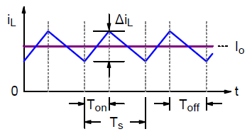
Figure 2. Inductor current waveform
Ripple current of inductor is defined as

Obviously, load current can be expressed as

A ripple factor can be defined as

When ripple factor is less than 2, the converter operates in continuous conduction mode (C.C.M), otherwise discontinuous conduction mode (D.C.M.). C.C.M. operation at full-load is more desired in an appropriate design of buck converters for its lower current stress in power semiconductors. Thus, only C.C.M. operation is discussed in this article.
Equation (8) can be expressed as voltage-related format
For a fixed inductor, the higher the input voltage, the higher ripple factor is. For a fixed input voltage, ripple factor is higher when the inductance is less. Higher ripple factor means more ripple current flows though capacitor. If same ripple voltage is required, bigger capacitor is necessary.
Area Product of an Inductor
As described above, the inductor will store energy during switch turn-on period, and release energy while switch turns off. Conceptually, the load current should pass through the inductor, such that enough area of winding wire is necessary. If lower ripple factor (or higher inductance) is designed, more winding turns is necessary, which leads to bigger size of inductor.
An index for measuring the inductor size called Area Product is introduced, which is the product of effective cross-section area of the core and area of winding window. The unit becomes m4 rather than m3 in volume. However, the area product is directly proportional to core volume.
From Faraday’s law, the relationship among inductance (L), peak current (ipk) and magnetic core can be derived as

where, ipk = Io + ½ DiL, N is the turns of winding and Bm is the maximum flux density of magnetic core. AC is the effective cross-section area of core.
From the winding, the following equation can be obtained.

where, Awr is the cross-section area of winding conductor, J is the current density of conductor. kw is the filling factor of core and Wa is the winding window area.
Combine (10) and (11), one can get

RMS current of an inductor can be arranged as its dc and ac terms.

Equation (12) can be re-written as
Figure 3 shows the normalized core size vs. ripple factor with respect to various duty cycle.
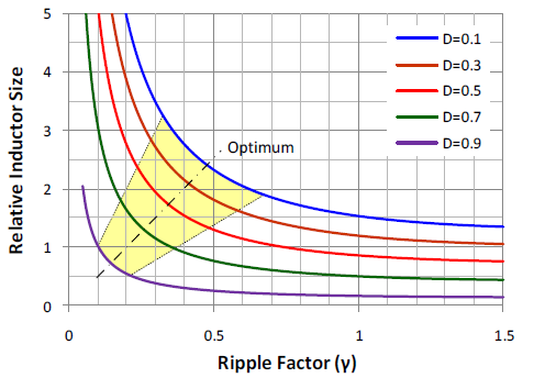
Figure 3. Relationship between ripple factor and inductor size with various duty cycle.
When ripple factor is in low area, core size will be dramatically increased and almost flat in high ripple factor. That means there exists an optimal range in near knee area. Basically, high ripple factor results in big filtering capacitor and vice versa. For example, as D = 0.3, ripple factor can be designed between 0.2 to 0.4, which results in a moderate core size and appropriate capacitor size.
Design Examples
A buck converter with 300kHz switching frequency has the following operating parameters,
Vin = 4 ~ 12V, Vout = 1.8V, Io = 6A, DVo = 10mV regarding to capacitance.
Assuming the power switch and freewheeling diode are ideal. Table 1 shows the inductance for traditional 30% ripple factor design, and optimal calculated values from proposed AP method is shown is Table 2.
Table 1. Conventional 30% ripple factor design
|
Input Voltage
(V)
|
Duty Cycle
|
Ripple Factor
|
Ripple Current (A)
|
Ripple Current RMS(A)
|
Inductance (mH)
|
|
4
|
0.30
|
0.3
|
1.80
|
0.52
|
1.56
|
|
8
|
0.15
|
0.3
|
1.80
|
0.52
|
1.89
|
|
12
|
0.1
|
0.3
|
1.80
|
0.52
|
2.00
|
Table 2. Optimal Inductance
|
Input Voltage
(V)
|
Duty Cycle
|
Optimal Ripple Factor
|
Ripple Current (A)
|
Ripple Current RMS(A)
|
Inductance (mH)
|
|
4
|
0.30
|
0.42
|
2.52
|
0.73
|
1.11
|
|
8
|
0.15
|
0.45
|
2.70
|
0.78
|
1.26
|
|
12
|
0.1
|
0.48
|
2.88
|
0.83
|
1.25
|
From Table 1, conventional approach has same designed ripple current, but larger inductor is needed for higher input voltage. While by applying AP method shown in Table 2, almost same inductances are calculated with different input voltage. However, the ripple current is higher for high input voltage. In practical high-frequency designs, POCAP or MLCC are often adopted as output capacitors, which have extremely low equivalent series resistance (ESR), such that ripple voltage requirement is easily satisfied.
Summary
A theoretical analysis between inductor size and ripple factor in Buck converter design is proposed. Optimal range of ripple factor can be obtained for different input voltages by AP method. It is a guideline for an optimal inductor design of a buck converter.